2009年4月22日星期三
vivi for QQ2440 board
project : vivi for QQ2440 develope board.
instruction : vivi(boot loader for arm) how to run before load system image.
(1) makefile of vivi.
(2) Head.S
(2.1) steppingstone (4k) (Nand flash can not execute directly but Nor flash and RAM).
(2.2) memory layout.
-- __________________________0x3400_0000 ( total: 64 M )
-- | ++++++ ViVi (1M) +++++++|
-- |_____________________|____0x33F0_0000 ( ViViRAM_BASE)
-- | ++++++ Heap (1M)++++++ |
-- |_____________________|____0x33E0_0000 ( Heap_BASE )
-- | ++++ MMU Table (16K)+++|
-- |_____________________|____0x33DF_C000 ( MMU_Table_BASE )
-- | ++ Priviate Data(16K x 3) ++|
-- |_____________________|__0x33DF_0000 ( ViVi_Priv_RAM_BASE )
-- | ++++++ Stack (32K) +++++|
-- |_____________________|____0x33DE_8000 ( STACK_BASE )
-- | ++++++ ++++++ ++++++ +|
-- |++++++ 61.90625 (M) ++++|
-- |++++++ ++++++ ++++++ + |
-- |____________________|____0x3000_0000 ( RAM_BASE )
(2.3) how the program jump to RAM from the startup code.
(2.3.1) The first step: (following text refer from S3C2440 datasheet)
( A ) S3C2440A boot code can be executed on an external NAND flash memory. In order to support NAND flash boot
loader, the S3C2440A is equipped with an internal SRAM buffer called ‘Steppingstone’. When booting, the first 4
KBytes of the NAND flash memory will be loaded into Steppingstone and the boot code loaded into Steppingstone
will be executed.
( B ) Auto boot: The boot code is transferred into 4-kbytes Steppingstone during reset. After the transfer, the boot
code will be executed on the Steppingstone.
(2.3.2) The second step:
( A ) Because of program can not execute from the media of Nandflash but Norflash, so must have to copy the vivi-self to
RAM when runing in steppingstone. The below figure was the first phase of vivi bootloadr(before go to main function).
-- __________________________
-- | ++++++++Reset target++++++++ |
-- |_________________________|
-- ----------------\|/
-- __________________________
-- | ++++++Disable watch dog +++++|
-- |_________________________|
-- ----------------\|/
-- __________________________
-- | +++++Disable all interupt ++++++|
-- |_________________________|
------------------ \|/
-- __________________________
-- |+++++Initialize system clock++++ |
-- |_________________________|
-- ----------------\|/
-- __________________________
-- |++++++ Memory setup++++++++ |
-- |_________________________|
------------------ \|/
-- __________________________
-- | +++++ All led on (indicate)+++++ |
-- |_________________________|
------------------ \|/
-- __________________________
-- | ++++++++Init UART++++++++ |
-- |_________________________|
------------------ \|/
-- _________________________
-- |+++++ Copy Vivi to RAM +++++ |
-- |________________________|
------------------ \|/
-- _________________________
-- | +++++Go to main func+++++++ |
-- |________________________|
--
( B ) Because the code be flash down into the Nandflash, and the PC must be reset 0x00000000 to starup.
-- ( 1 ) Linker option:
-- link script file for arm-linux-ld
-- "LINKFLAGS = -Tarch/vivi.lds" -Bstatic from the $(TOPDIR)/Makefile
-- The comtent of vivi.lds as following:
-- SECTIONS {
-- . = 0x33f00000;
-- .text : { *(.text) }
-- .data ALIGN(4) : { *(.data) }
-- .bss ALIGN(4) : { *(.bss) *(COMMON) }
-- }
--
-- The 0x33f00000 is the start address create by arm-linux-ld.
-- You can use tool arm-linux-objdump to dump the elf file with option "-D"
-- the below fragement as the example:
--
-- $ /cygdrive/c/Cygnus/arm-tools/bin/arm-uclibc-objdump.exe -D d:/vivi-elf
-- d:/vivi-elf: file format elf32-littlearm
-- Disassembly of section .text:
-- 33f00000 <>:
-- 33f00000: ea00000b b 33f00034 <>
-- 33f00004 <>:
-- 33f00004: ea000099 b 33f00270 <>
-- 33f00008 <>:
-- 33f00008: ea000099 b 33f00274 <>
-- and so on ...
--
-- ( 2 ) Reset target:
-- Because the Code be localed from address 0x00000000, so at the beginning the all
-- branch instruction (as like B, BL ) will jump to the relative address.
-- For exmaple:
$ /cygdrive/c/Cygnus/arm-tools/bin/arm-uclibc-objdump.exe -D d:/vivi-elf
Disassembly of section .text:
33f00000 <>:
33f00000: ea00000b b 33f00034 <>
B to instruction_address+8+4*offset
-------------------------------------------------------------------------------------------------------------
| 31 30 29 28 | 27 26 25 24 | 23 22 21 20 19 18 17 16 15 14 13 12 11 10 9 8 7 6 5 4 3 2 1 0 |
-------------------------------------------------------------------------------------------------------------
| ++cond++ | ++1 0 1 0++ | ++++++++ signed 24-bit branch offset +++++++++++++|
-------------------------------------------------------------------------------------------------------------
ea00000b:
-------------------------------------------------------------------------------------------------------------
| ++ 1110++ |++ 1010 ++ | +++0000_0000_0000_0000_0000_1011 (0x34) ++++|
-------------------------------------------------------------------------------------------------------------
According to formula "instruction_address+8+4*offset", so the current PC be load in relative address:
(instruction_address: PC=0x00000000) + 8 + 4 * (offset: 1011=11) = 0x34
-- ( 3 ) Copy Vivi to RAM:
-- We are now not describe the Copy code here, we will intruduce the PC register how to jumping
-- at RAM area from current SARM (steppingstone.)
-- Following fragment is the disassembling code by the "arm-linux-objdump -D" command:
==================================================================================================
@ fragment code of head.S
@ jump to ram
ldr r1, =on_the_ram
add pc, r1, #0
nop
nop
1: b 1b @ infinite loop
on_the_ram:
@ get read to call C functions
ldr sp, DW_STACK_START @ setup stack pointer
mov fp, #0 @ no previous frame, so fp=0
mov a2, #0 @ set argv to NULL
bl main @ call main
mov pc, #FLASH_BASE @ otherwise, reboot
-+-+-+-+-+-+-+-+-+-+-+-+-+-+-+-+-+-+-+-+-+-+-+-+-+-+-+-+-+-+-+-+-+-+-+-+-+-+-+-+-+-+-+-+-+-+-+-+-+
.align 4
SerBase:
#if defined(CONFIG_SERIAL_UART0)
.long UART0_CTL_BASE
#elif defined(CONFIG_SERIAL_UART1)
.long UART1_CTL_BASE
#elif defined(CONFIG_SERIAL_UART2)
.long UART2_CTL_BASE
#error not defined base address of serial
#endif
the end of file "head.S"
==================================================================================================
33f000d8: e59f1230 ldr r1, [pc, #560] ; 33f00310 <>
33f000dc: e281f000 add pc, r1, #0 ; 0x0
33f000e0: e1a00000 nop (mov r0,r0)
33f000e4: e1a00000 nop (mov r0,r0)
33f000e8: eafffffe b 33f000e8 <>
33f000ec <>:
33f000ec: e59fd200 ldr sp, [pc, #512] ; 33f002f4 <>
33f000f0: e3a0b000 mov fp, #0 ; 0x0
33f000f4: e3a01000 mov r1, #0 ; 0x0
33f000f8: eb000405 bl 33f01114 <>
33f000fc: e3a0f000 mov pc, #0 ; 0x0
-+-+-+-+-+-+-+-+-+-+-+-+-+-+-+-+-+-+-+-+-+-+-+-+-+-+-+-+-+-+-+-+-+-+-+-+-+-+-+-+-+-+-+-+-+-+-+-+-+
33f00300 <>:
33f00300: 50000000 andpl r0, r0, r0
33f00304: 000007ff streqd r0, [r0], -pc
33f00308: 0007f021 andeq pc, r7, r1, lsr #32
33f0030c: 000055aa andeq r5, r0, sl, lsr #11
33f00310: 33f000ec mvnccs r0, #236 ; 0xec
33f00314: 00007770 andeq r7, r0, r0, ror r7
33f00318: 33f00000 mvnccs r0, #0 ; 0x0
33f0031c: 00000245 andeq r0, r0, r5, asr #4
==================================================================================================
-- First step: suppose now execute instruction "ldr r1, [pc, #560]" and so we had known the PC now be load with 0x000000e0 since
-- ARM process support line pipe, and now we can work out the r1 = mem[0x000000e0 + #560(dec)] = mem[0x00000310], now we can look at
-- the content of offset 0x00000310 from mem is 33f000ec, therefore r1 = 0x33f000ec, then the next instruction "add pc, r1, #0"
-- is make the PC go to RAM ( PC=0x33f000ec ).
--
-- Second step: why the value of offset 33f00310 from mem is the value of PC jumping, we first look at the C code: the lable "on_the_ram"
-- is create by arm-linux-as assembler and generate the code like this: "on_the_ram: .word 33f000ec" and lay it at address: 0x33f00310.
-- so can see the line "33f00310: 33f000ec mvnccs r0, #236 ; 0xec" is the dissembling code of "on_the_ram: .word 33f000ec",
-- and be place at the end of ROM code. this is genrated by assembler automatically.
--
-- Third step: You can enable the switch "CONFIG_DEBUG_LL" for debugging via serial port.
--
-- Done!
--
(3) others for vivi
2009年4月14日星期二
debugging with Jlink under keil
project : debugging with Jlink under keil
instuction: jlinker settings for QQ2440 board under keil IDE
(1) Firstly, modify the scatter files as following( locate it start at SDRAM: 0x30000000):
scatter file:
; *************************************************************
; *** Scatter-Loading Description File generated by uVision ***
; *************************************************************
LR_ROM1 0x30000000 { ; load region size_region
RO +0 { ; load address = execution address
2440init.o (+RO,+First)
*(InRoot$$Sections)
.ANY (+RO)
}
RW +0 { ; RW data
.ANY (+RW)
}
ZI +0 { ; ZI data
.ANY (+ZI)
}
}
=================================================================
(2) Do not enable the item "Run to main()", because when the target reset, the PC value is 0x00000000, so will change it to 0x30000000 to run.(if not, it can not change the PC register value.)
(3) enter into "SEGGER J-Link RDI V4.02 Congiuration" Dialog and setting as below.
(3.1) General page: USB --> Device 0
(3.2) Init page: macro file as following:
filename: QQ2440.setup:
===================================================================
/*********************************************************************
*
* Macro file for J-LINK RDI
*
**********************************************************************
* File: QQ2440.setup
* Purpose: Setup for S3C2440 chip
**********************************************************************
*/
Write32(0x53000000, 0x00000000);
Write32(0x4A000008, 0xFFFFFFFF);
Write32(0x4A00001C, 0x000007FF);
Write32(0x53000000, 0x00000000);
Write32(0x56000050, 0x000055AA);
Write32(0x4C000014, 0x00000007);
Write32(0x4C000000, 0x00FFFFFF);
Write32(0x4C000004, 0x00061012);
Write32(0x4C000008, 0x00040042);
Write32(0x48000000, 0x22111120);
Write32(0x48000004, 0x00002F50);
Write32(0x48000008, 0x00000700);
Write32(0x4800000C, 0x00000700);
Write32(0x48000010, 0x00000700);
Write32(0x48000014, 0x00000700);
Write32(0x48000018, 0x0007FFFC);
Write32(0x4800001C, 0x00018005);
Write32(0x48000020, 0x00018005);
Write32(0x48000024, 0x008E0459);
Write32(0x48000028, 0x00000032);
Write32(0x4800002C, 0x00000030);
Write32(0x48000030, 0x00000030);
===================================================================
(3.3) JTAG page: JTAG speed --> 12000 kHz
(3.4) Flash page: Disable Flash programming.
(3.5) Breakpoints page: Enable Use software breakpoints.
(3.6) CPU page: Enable Allow instruction set simulation, Little endian. Reset Normal.
(3.7) Log page: None.
Done! Good Luck!
2009年4月13日星期一
j-flash setting for QQ2440
project : J-Flash ARM V4.02 setting for QQ2440 borad.
instruction: use J-flash ARM software flash device of QQ2440.
(1) create project named "S3C2440.jflash" for QQ2440 device.
(2) menu: [Options]-->[option settings]
|-- Gneral page: Connectioin to J-link --> USB
|-- Target Interface page: default
|-- CPU page: Core --> ARM9, Little endian, Use target RAM(faster)-->Addr:40000000 4KB
-----| Use following init sequence start |-----
##-------Action--------Value0------Value1
00----Write 32bit---0x53000000---0x00000000
01----Write 32bit---0x4A000008---0xFFFFFFFF
02----Write 32bit---0x4A00001C---0x000007FF
03----Write 32bit---0x53000000---0x00000000
04----Write 32bit---0x56000050---0x000055AA
05----Write 32bit---0x4C000014---0x00000007
06----Write 32bit---0x4C000000---0x00FFFFFF
07----Write 32bit---0x4C000004---0x00061012
08----Write 32bit---0x4C000008---0x00040042
09----Write 32bit---0x48000000---0x22111120
10----Write 32bit---0x48000004---0x00002F50
11----Write 32bit---0x48000008---0x00000700
12----Write 32bit---0x4800000C---0x00000700
13----Write 32bit---0x48000010---0x00000700
14----Write 32bit---0x48000014---0x00000700
15----Write 32bit---0x48000018---0x0007FFFC
16----Write 32bit---0x4800001C---0x00018005
17----Write 32bit---0x48000020---0x00018005
18----Write 32bit---0x48000024---0x008E0459
19----Write 32bit---0x48000028---0x00000032
20----Write 32bit---0x4800002C---0x00000030
20----Write 32bit---0x48000030---0x00000030
-----| Use following init sequence end |-----
|-- Flash page: Base Addr: 0000000, Organization: 16 Bits x 1 Chip(s), Select flash device: Am29LV160DB, disable"Check manufacturer flash ID and Check product flash ID
|-- Production page: Erase, Program and Verify enable.
(NOTE: when you can not flash device, maybe should reset target board will be better.)
2009年4月12日星期日
H-Jtag setting for QQ2440 board
project : H-Jtag setting
instruction: this setting just for QQ2440 board.
H-Jtag Server setting:
(1)main menu: [settings]->[USB/LPT selection] choose LPT;
(2)main menu: [settings]->[LPT Jtag setting]
|-- Jtag Selection: User Defined
|-- TCK Control: MAX/1
|-- User Defined Pin Assignment
------|-- TMS: Pin4 D2
------|-- TCK: Pin2 D0
------|-- TDI: Pin3 D1
------|-- TD0: Pin11 busy
------|-- nTRST: NO TAP RST
------|-- nSRST: NO SYS RST
if you want more detail about these, pls get it from its attched book <<书名:H-JTAG USER MANUAL>>, following is fragment of its instruction.
====================================================================
4.6.4 LPT JTAG Setting
The LPT based JTAG controller does not have a fixed schematic, even for WIGGLER and SDT-JTAG. Some
JTAG emulator comes with nSRST, while others don’t have. Some JTAG emulator provides separate nSRST and
nTRST, while others connected them together. To support different LPT based JTAG emulators, H-JTAG provides
a flexible configuration interface. What user needs to do is tell H-Jtag exactly how the JTAG emulator is
connected to LPT.
The LPT provides 8 data bits, D0-D7, as output and several status bits as input. The data bits can be used as
JTAG output signals, TMS, TCK, TDI, nSRST and nTRST. Any one of the status bits can be used as input to
sample TDO. The JTAG configuration is to specify how the JTAG signals are connected with the data bits and
status bits. On some JTAG emulator, the nSRST and nTRST are inverted. These also need to be specified in the
JTAG configuration.
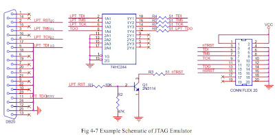
Next, let’s look at an illustrative example. The schematic of the JTAG emulator used in the example is show
in Fig 4-7. The connection between LPT and JTAG can be obtained from the schematic and is listed in following
table. Please note that the nTRST signal is inverted and no nSRST signal is provided.
--------------------------------------
TMS ------>> LPT D1 (PIN3)
TCK ------>> LPT D2 (PIN4)
TDI ------>> LPT D3 (PIN5)
TDO ------>> LPT BUSY (PIN11)
nTRST ---->> LPT D0 (PIN2) INVERTED
nSRST <<---- X NOT AVAILABLE
--------------------------------------
picture : H-jtag.bmp
===========================================================
(3) initial register before flash. main menu: [Script]-->[init Script] choose following file:FriendlyARM2440.his
file: FriendlyARM2440.his
=================================================== ========
Setmem+32-Bit+0x53000000+0x00000000 ;WTCON
Setmem+32-Bit+0x4A000008+0xFFFFFFFF ;INTMSK
Setmem+32-Bit+0x4A00001C+0x000007FF ;INTSUBMSK
Setmem+32-Bit+0x53000000+0x00000000 ;WTCON
Setmem+32-Bit+0x56000050+0x000055AA ;GPFCON
Setmem+32-Bit+0x4C000014+0x00000007 ;CLKDIVN
Setmem+32-Bit+0x4C000000+0x00FFFFFF ;LOCKTIME
Setmem+32-Bit+0x4C000004+0x00061012 ;MPLLCON
Setmem+32-Bit+0x4C000008+0x00040042 ;UPLLCON
Setmem+32-Bit+0x48000000+0x22111120 ;BWSCON
Setmem+32-Bit+0x48000004+0x00002F50 ;BANKCON0
Setmem+32-Bit+0x48000008+0x00000700 ;BANKCON1
Setmem+32-Bit+0x4800000C+0x00000700 ;BANKCON2
Setmem+32-Bit+0x48000010+0x00000700 ;BANKCON3
Setmem+32-Bit+0x48000014+0x00000700 ;BANKCON4
Setmem+32-Bit+0x48000018+0x0007FFFC ;BANKCON5
Setmem+32-Bit+0x4800001C+0x00018005 ;BANKCON6
Setmem+32-Bit+0x48000020+0x00018005 ;BANKCON7
Setmem+32-Bit+0x48000024+0x008E0459 ;REFRESH
Setmem+32-Bit+0x48000028+0x00000032 ;BANKSIZE
Setmem+32-Bit+0x4800002C+0x00000030 ;MRSRB6
Setmem+32-Bit+0x48000030+0x00000030 ;MRSRB7
---------------------------------------------------------------------
(NOTE: Pls choose [Enable Auto Init] item, otherwise can not halt to main function when you use F5 for debugging with target borad.)
(4) H-Flasher configure
|-- Flash Selection : AMD-->AM29LV160DB
|-- Configuration
------|-- Flash Width x Chip : 16-Bitx1-Chip
------|-- Flash Start Address: 0x00000000
------|-- RAM Start Address : 0x30000000
|-- Programming
------|-- Check : if check okay, so everything goes all right. if not, maybe you can reset target will help you resolve this problem.
------|-- Type : (1)Auto Flash Download-->for debug inline (2)intel Hex format-->flash Hex file (3) Plain Binary Format-->flash bin file.
instruction: this setting just for QQ2440 board.
H-Jtag Server setting:
(1)main menu: [settings]->[USB/LPT selection] choose LPT;
(2)main menu: [settings]->[LPT Jtag setting]
|-- Jtag Selection: User Defined
|-- TCK Control: MAX/1
|-- User Defined Pin Assignment
------|-- TMS: Pin4 D2
------|-- TCK: Pin2 D0
------|-- TDI: Pin3 D1
------|-- TD0: Pin11 busy
------|-- nTRST: NO TAP RST
------|-- nSRST: NO SYS RST
if you want more detail about these, pls get it from its attched book <<书名:H-JTAG USER MANUAL>>
====================================================================
4.6.4 LPT JTAG Setting
The LPT based JTAG controller does not have a fixed schematic, even for WIGGLER and SDT-JTAG. Some
JTAG emulator comes with nSRST, while others don’t have. Some JTAG emulator provides separate nSRST and
nTRST, while others connected them together. To support different LPT based JTAG emulators, H-JTAG provides
a flexible configuration interface. What user needs to do is tell H-Jtag exactly how the JTAG emulator is
connected to LPT.
JTAG output signals, TMS, TCK, TDI, nSRST and nTRST. Any one of the status bits can be used as input to
sample TDO. The JTAG configuration is to specify how the JTAG signals are connected with the data bits and
status bits. On some JTAG emulator, the nSRST and nTRST are inverted. These also need to be specified in the
JTAG configuration.
in Fig 4-7. The connection between LPT and JTAG can be obtained from the schematic and is listed in following
table. Please note that the nTRST signal is inverted and no nSRST signal is provided.
--------------------------------------
TMS ------>> LPT D1 (PIN3)
TCK ------>> LPT D2 (PIN4)
TDI ------>> LPT D3 (PIN5)
TDO ------>> LPT BUSY (PIN11)
nSRST <<---- X NOT AVAILABLE
--------------------------------------
picture : H-jtag.bmp

(3) initial register before flash. main menu: [Script]-->[init Script] choose following file:FriendlyARM2440.his
file: FriendlyARM2440.his
Setmem+32-Bit+0x4A000008+0xFFFFFFFF ;INTMSK
Setmem+32-Bit+0x4A00001C+0x000007FF ;INTSUBMSK
Setmem+32-Bit+0x53000000+0x00000000 ;WTCON
Setmem+32-Bit+0x56000050+0x000055AA ;GPFCON
Setmem+32-Bit+0x4C000014+0x00000007 ;CLKDIVN
Setmem+32-Bit+0x4C000000+0x00FFFFFF ;LOCKTIME
Setmem+32-Bit+0x4C000004+0x00061012 ;MPLLCON
Setmem+32-Bit+0x4C000008+0x00040042 ;UPLLCON
Setmem+32-Bit+0x48000000+0x22111120 ;BWSCON
Setmem+32-Bit+0x48000004+0x00002F50 ;BANKCON0
Setmem+32-Bit+0x48000008+0x00000700 ;BANKCON1
Setmem+32-Bit+0x4800000C+0x00000700 ;BANKCON2
Setmem+32-Bit+0x48000010+0x00000700 ;BANKCON3
Setmem+32-Bit+0x48000014+0x00000700 ;BANKCON4
Setmem+32-Bit+0x48000018+0x0007FFFC ;BANKCON5
Setmem+32-Bit+0x4800001C+0x00018005 ;BANKCON6
Setmem+32-Bit+0x48000020+0x00018005 ;BANKCON7
Setmem+32-Bit+0x48000024+0x008E0459 ;REFRESH
Setmem+32-Bit+0x48000028+0x00000032 ;BANKSIZE
Setmem+32-Bit+0x4800002C+0x00000030 ;MRSRB6
Setmem+32-Bit+0x48000030+0x00000030 ;MRSRB7
---------------------------------------------------------------------
(NOTE: Pls choose [Enable Auto Init] item, otherwise can not halt to main function when you use F5 for debugging with target borad.)
(4) H-Flasher configure
|-- Flash Selection : AMD-->AM29LV160DB
|-- Configuration
------|-- Flash Width x Chip : 16-Bitx1-Chip
------|-- Flash Start Address: 0x00000000
------|-- RAM Start Address : 0x30000000
|-- Programming
------|-- Check : if check okay, so everything goes all right. if not, maybe you can reset target will help you resolve this problem.
------|-- Type : (1)Auto Flash Download-->for debug inline (2)intel Hex format-->flash Hex file (3) Plain Binary Format-->flash bin file.
2009年4月11日星期六
VMware Network Configure
project : Vmware Network
instruction: because of my network have bind the MAC number and IP address, so if make the both host and vmware system
able to connect to Internet, it must tweak vmware network configure for it.
(1) case analyze : my Vmware system have installed Redhead 9.0 and host sytem is winXP, make the both can connect to Internet.
(2) Vmware Configure: Vmware provides 3 types of networking, as bellow:
BRIGE : it's equal to make the virtual machine connect Internet as PC host.(make the network adapter work as promiscuous mode)
but it just only use differ IP for both host and virtual machine.
NAT : NAT gives a virtual machine access to network resources using the host computer's IP address. It is easy to understand that
the NAT networking in VM if you have an experience of NAT networking configuration. The subnet in the virtual machine is
different of host's subnet. Then the NAT map was done by the virtual hardware VM-net8. (so i choose this mode for mine)
Host-Only : this mode just only for virtual machine connect to Host PC, and you must configure the virtual machine IP address the
same sub-net as VMnet1 of your host.
(Note: Don't change the VMnet1 and VMnet8's ip address, if changed it doesn't not work at all.)
(3) Use DHCP connect to Internet from my virtual machine, but it doesn't work at all, and use "ping www.sina.com" in return
"ping: unknown host www.sina.com", but can ping my host PC, so it should configure the DNS for my virtual machine. after config DNS done,
everything goes all right.
(4) fllowing is my private configure for my virtual machine (redhat9.0)
host system: window XP
ipconfig /all
Ethernet adapter VMware Network Adapter VMnet8:
Connection-specific DNS Suffix . :
Description . . . . . . . . . . . : VMware Virtual Ethernet Adapter for VMnet8
Physical Address. . . . . . . . . : 00-50-56-C0-00-08
Dhcp Enabled. . . . . . . . . . . : No
IP Address. . . . . . . . . . . . : 192.168.115.1
Subnet Mask . . . . . . . . . . . : 255.255.255.0
Default Gateway . . . . . . . . . :
Ethernet adapter VMware Network Adapter VMnet1:
Connection-specific DNS Suffix . :
Description . . . . . . . . . . . : VMware Virtual Ethernet Adapter for VMnet1
Physical Address. . . . . . . . . : 00-50-56-C0-00-01
Dhcp Enabled. . . . . . . . . . . : No
IP Address. . . . . . . . . . . . : 192.168.142.1
Subnet Mask . . . . . . . . . . . : 255.255.255.0
Default Gateway . . . . . . . . . :
===========================================================================================
virtual machine : redhat 9.0
config virtual machine IP address:
;;my virtual machine is Redhat
IP Address. . . . . . . . . . . . : 192.168.115.*
Subnet Mask . . . . . . . . . . . : 255.255.255.0
Default Gateway . . . . . . . . . : 192.168.115.2
(Note: Default Gateway should be 2)
===========================================================================================
QQ2440 project migrate
project : QQ2440 arm broad
instuction: ADS1.2 project migrate to keil for arm project (RV3.1)
(1) copy source code from ADS1.2 project to keil project.
ADS1.2 project list: | keil project list:
2440test
|
|-- inc/*
|-- src/*
|-- 2440test.mcp
|-- others | |-- others
2440test_keil
|
|-- inc/*
|-- src/*
|-- 2440test_keil.Uv2
|-- others
(2) liner error:
---------------------------------------------------------------------------------------------------------------------------------
test_keil.axf: Error: L6238E: 2440init.o(Init) contains invalid call from '~PRES8' function to 'REQ8' function Main.
---------------------------------------------------------------------------------------------------------------------------------
resovle method: (forward from http://infocenter.arm.com/help/index.jsp?topic=/com.arm.doc.faqs/ka3556.html)
---------------------------------------------------------------------------------------------------------------------------------
Solutions
There are two possible approaches to dealing with this issue:
1) If you have access to all your source code and are allowed to rebuild it
In this case you should rebuild all your objects/libraries using the latest version of the compilation tools.
Note that if you have any assembler files, you will need to:
i) check that all instructions preserve 8-byte stack alignment, and if necessary, correct them.
e.g. change:
STMFD sp!, {r0-r3, lr} ; push an odd number of registers
to:
STMFD sp!, {r0-r3, r12, lr} ; push an even number of registers
and:
ii) add the PRESERVE8 directive to the top of each assembler file.
e.g. change:
AREA Init, CODE, READONLY
to:
PRESERVE8
AREA Init, CODE, READONLY
(the PRES8 attribute applies to the whole object, not just the code section).
2) If you cannot rebuild all of your source code
If you have any legacy objects/libraries that cannot be rebuilt, either because you do not have the source code,
or because the old objects must not be rebuilt (e.g. for qualification/certification reasons), then you must inspect
the legacy objects to check whether they preserve 8-byte alignment or not. Use "fromelf -c" to disassemble the object code.
C/C++ code compiled with ADS 1.1 or later will normally preserve 8-byte alignment, but assembled code will not.
If your objects do indeed preserve 8-byte alignment, then the linker error L6238E can be suppressed with the use
of "--diag_suppress 6238" on the linker command line. By using this, you are effectively saying "I guarantee that
these objects are PRES8". The linker warning L6306W is suppressible with "--diag_suppress 6306".
If you are linking with legacy objects/libraries then you should also read the information on the option "--apcs /adsabi"
in the FAQ entry "Are legacy ADS objects/libraries compatible with RVCT 2.0 ?".
---------------------------------------------------------------------------------------------------------------------------------
(3) project setting for keil
(3.1) Choose the linker page.
(3.2) Disable the item: Use the memory layout from the target dialog.
(3.3) use scatter file for linker, and its content as following:
; *************************************************************
; *** Scatter-Loading Description File generated by uVision ***
; *************************************************************
LR_ROM1 0x00000000 { ; load region size_region
RO +0 { ; load address = execution address
2440init.o (+RO,+First)
*(InRoot$$Sections)
.ANY (+RO)
}
RW +0x30000000 { ; RW data
.ANY (+RW)
}
ZI +0 { ; ZI data
.ANY (+ZI)
}
}
(Note: If you are using a scatter-loading description file, the output section symbols in Table 1.0 are undefined
so use exec_section_name can genrate synbol like Image$$RO$$Base by liker.)
Table 1.0
---------------------------------------------------------------------------------------------------------------------------------
Symbol Section type Description
---------------------------------------------------------------------------------------------------------------------------------
Image$$RO$$Base Output Address of the start of the RO output section.
Image$$RO$$Limit Output Address of the first byte beyond the end of the RO output section.
Image$$RW$$Base Output Address of the start of the RW output section.
Image$$RW$$Limit Output Address of the byte beyond the end of the ZI output section.
(The choice of the end of the ZI region rather than the end of the RW region is to maintain compatibility with legacy code.)
Image$$ZI$$Base Output Address of the start of the ZI output section.
Image$$ZI$$Limit Output Address of the byte beyond the end of the ZI output section
----------------------------------------------------------------------------------------------------------------------------------
(3.4) you can get the linker option from the "linker control string" district as below:
----------------------------------------------------------------------------------------------------------------------------------
liker option:
----------------------------------------------------------------------------------------------------------------------------------
--autoat --summary_stderr --info summarysizes --map --xref --callgraph --symbols --info sizes
--info totals --info unused --info veneers --list ".\test_keil.map" -o "2440test_keil.axf"
----------------------------------------------------------------------------------------------------------------------------------
(4) download the "2440test_keil.hex" to broad by H-Flasher.
订阅:
博文 (Atom)
