instruction: this setting just for QQ2440 board.
H-Jtag Server setting:
(1)main menu: [settings]->[USB/LPT selection] choose LPT;
(2)main menu: [settings]->[LPT Jtag setting]
|-- Jtag Selection: User Defined
|-- TCK Control: MAX/1
|-- User Defined Pin Assignment
------|-- TMS: Pin4 D2
------|-- TCK: Pin2 D0
------|-- TDI: Pin3 D1
------|-- TD0: Pin11 busy
------|-- nTRST: NO TAP RST
------|-- nSRST: NO SYS RST
if you want more detail about these, pls get it from its attched book <<书名:H-JTAG USER MANUAL>>
====================================================================
4.6.4 LPT JTAG Setting
The LPT based JTAG controller does not have a fixed schematic, even for WIGGLER and SDT-JTAG. Some
JTAG emulator comes with nSRST, while others don’t have. Some JTAG emulator provides separate nSRST and
nTRST, while others connected them together. To support different LPT based JTAG emulators, H-JTAG provides
a flexible configuration interface. What user needs to do is tell H-Jtag exactly how the JTAG emulator is
connected to LPT.
JTAG output signals, TMS, TCK, TDI, nSRST and nTRST. Any one of the status bits can be used as input to
sample TDO. The JTAG configuration is to specify how the JTAG signals are connected with the data bits and
status bits. On some JTAG emulator, the nSRST and nTRST are inverted. These also need to be specified in the
JTAG configuration.
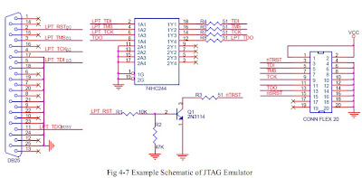
in Fig 4-7. The connection between LPT and JTAG can be obtained from the schematic and is listed in following
table. Please note that the nTRST signal is inverted and no nSRST signal is provided.
--------------------------------------
TMS ------>> LPT D1 (PIN3)
TCK ------>> LPT D2 (PIN4)
TDI ------>> LPT D3 (PIN5)
TDO ------>> LPT BUSY (PIN11)
nSRST <<---- X NOT AVAILABLE
--------------------------------------
picture : H-jtag.bmp

(3) initial register before flash. main menu: [Script]-->[init Script] choose following file:FriendlyARM2440.his
file: FriendlyARM2440.his
Setmem+32-Bit+0x4A000008+0xFFFFFFFF ;INTMSK
Setmem+32-Bit+0x4A00001C+0x000007FF ;INTSUBMSK
Setmem+32-Bit+0x53000000+0x00000000 ;WTCON
Setmem+32-Bit+0x56000050+0x000055AA ;GPFCON
Setmem+32-Bit+0x4C000014+0x00000007 ;CLKDIVN
Setmem+32-Bit+0x4C000000+0x00FFFFFF ;LOCKTIME
Setmem+32-Bit+0x4C000004+0x00061012 ;MPLLCON
Setmem+32-Bit+0x4C000008+0x00040042 ;UPLLCON
Setmem+32-Bit+0x48000000+0x22111120 ;BWSCON
Setmem+32-Bit+0x48000004+0x00002F50 ;BANKCON0
Setmem+32-Bit+0x48000008+0x00000700 ;BANKCON1
Setmem+32-Bit+0x4800000C+0x00000700 ;BANKCON2
Setmem+32-Bit+0x48000010+0x00000700 ;BANKCON3
Setmem+32-Bit+0x48000014+0x00000700 ;BANKCON4
Setmem+32-Bit+0x48000018+0x0007FFFC ;BANKCON5
Setmem+32-Bit+0x4800001C+0x00018005 ;BANKCON6
Setmem+32-Bit+0x48000020+0x00018005 ;BANKCON7
Setmem+32-Bit+0x48000024+0x008E0459 ;REFRESH
Setmem+32-Bit+0x48000028+0x00000032 ;BANKSIZE
Setmem+32-Bit+0x4800002C+0x00000030 ;MRSRB6
Setmem+32-Bit+0x48000030+0x00000030 ;MRSRB7
---------------------------------------------------------------------
(NOTE: Pls choose [Enable Auto Init] item, otherwise can not halt to main function when you use F5 for debugging with target borad.)
(4) H-Flasher configure
|-- Flash Selection : AMD-->AM29LV160DB
|-- Configuration
------|-- Flash Width x Chip : 16-Bitx1-Chip
------|-- Flash Start Address: 0x00000000
------|-- RAM Start Address : 0x30000000
|-- Programming
------|-- Check : if check okay, so everything goes all right. if not, maybe you can reset target will help you resolve this problem.
------|-- Type : (1)Auto Flash Download-->for debug inline (2)intel Hex format-->flash Hex file (3) Plain Binary Format-->flash bin file.

没有评论:
发表评论